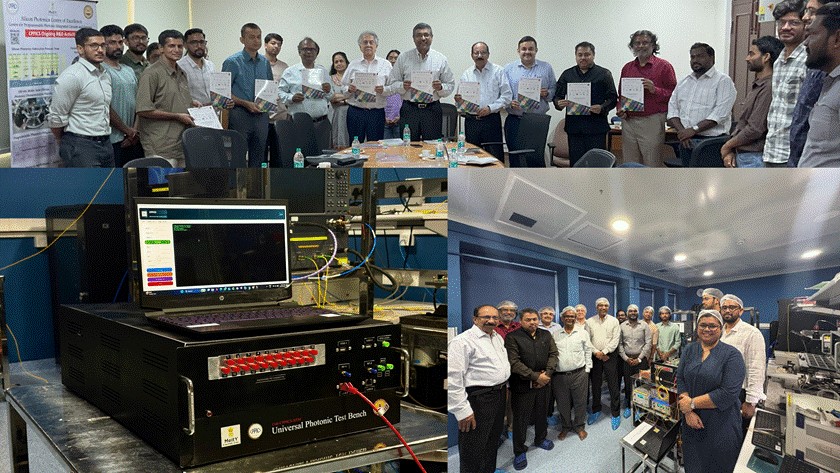
CHENNAI, APRIL 24: The Government of India on Friday launched two indigenously developed silicon photonics technology solutions at Indian Institute of Technology Madras, aimed at advancing domestic capabilities in photonics chip design and testing.
The launch was carried out by S. Krishnan, Secretary, Ministry of Electronics and Information Technology (MeitY), in the presence of senior officials and researchers. The technologies include a Silicon Photonics Process Design Kit (PDK) for chip manufacturing and a Universal Programmable Photonic Integrated Circuit (PPIC) Test Engine, both developed at the MeitY-supported Centre of Excellence for Silicon Photonics at IIT Madras.
Officials said the development marks a step toward strengthening India’s technological capabilities in silicon photonics and will function as a shared national facility for research and development across industry, academia and defence sectors.
According to MeitY, the Silicon Photonics PDK includes a library of more than 50 verified components, enabling design and development of photonic integrated circuits within the country. The Universal PPIC Test Engine is an automated platform designed for characterisation of photonic and optoelectronic modules across multiple applications.
Speaking at the event, Krishnan said the progress in silicon photonics aligns with global standards and highlighted the need for establishing fabrication facilities under the India Semiconductor Mission to complement research and development efforts.
Additional Secretary MeitY and CEO of the India Semiconductor Mission, Amitesh Sinha, said the technology has applications in both classical and quantum domains and could be supported under future phases of semiconductor initiatives for further development and commercialization.
Officials also announced the next phase of work under the centre, which will include enabling multi-project wafer fabrication runs and expanding capabilities for testing, packaging and module characterisation.
The Centre of Excellence operates on a Product Research, Development and Manufacturing model using CMOS-compatible silicon photonics technology, with international and domestic partners supporting fabrication and packaging processes.
The government said the initiative is part of broader efforts to build self-reliance in semiconductor and photonics technologies and to strengthen India’s position in advanced electronics manufacturing. (PIB)
Comments are closed.